

/ News
Patterning defect-free nanocrystal films with nanometer resolution
Films made of semiconductor nanocrystals — tiny crystals measuring just a few billionths of a meter across — are seen as a promising new material for a wide range of applications. Nanocrystals could be used in electronic or photonic circuits, detectors for biomolecules, or the glowing pixels on high-resolution display screens. They also hold promise for more efficient solar cells.
The size of a semiconductor nanocrystal determines its electrical and optical properties. But it’s very hard to control the placement of nanocrystals on a surface in order to make structurally uniform films. Typical nanocrystal films also have cracks that limit their usefulness and make it impossible to measure the fundamental properties of these materials.
Now, researchers at MIT say they have found ways of making defect-free patterns of nanocrystal films where the shape and position of the films are controlled with nanoscale resolution, potentially opening up a significant area for research and possible new applications.
“We’ve been trying to understand how electrons move in arrays of these nanocrystals,” which has been difficult with limited control over the formation of the arrays, says physicist Marc Kastner, the Donner Professor of Science, dean of MIT’s School of Science and senior author of a paper published online in the journal Nano Letters.
The work builds on research by Moungi Bawendi, the Lester Wolfe Professor of Chemistry at MIT and a co-author of this paper, who was one of the first researchers to precisely control nanocrystal production. Such control made it possible, among other things, to produce materials that glow, or fluoresce, in a range of different colors based on their sizes — even though they are all made of the same material.
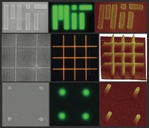
In the initial phases of the new work, postdoc Tamar Mentzel produced nanoscale patterns that emit invisible infrared light. But working on such systems is tedious, since each fine-tuning has to be checked using time-consuming electron microscopy. So when Mentzel succeeded in getting semiconductor nanocrystal patterns to glow with visible light, making them visible through an optical microscope, it meant that the team could greatly speed the development of the new technology. “Even though the nanoscale patterns are below the resolution limit of the optical microscope, the nanocrystals act as a light source, rendering them visible,” Mentzel says.
The electrical conductivity of the researchers’ defect-free films is roughly 180 times greater than that of the cracked films made by conventional methods. In addition, the process developed by the MIT team has already made it possible to create patterns on a silicon surface that are just 30 nanometers across — about the size of the finest features possible with present manufacturing techniques.
The process is unique in producing such tiny patterns of defect-free films, Mentzel says. “The trick was to get the film to be uniform, and to stick” to the silicon dioxide substrate, Kastner adds. That was achieved by leaving a thin layer of polymer to coat the surface before depositing the layer of nanocrystals on top of it. The researchers conjecture that tiny organic molecules on the surface of the nanocrystals help them bind to the polymer layer.
Such nanocrystal patterns could have many applications, Kastner says. Because these nanocrystals can be tuned not only to emit but also to absorb a wide spectrum of colors of light, they could enable a new kind of broad-spectrum solar cell, he says.
But Kastner and Mentzel’s personal interest has more to do with basic physics: Since the minuscule crystals behave almost like oversized atoms, the researchers aim to use the arrays to study fundamental processes of solids, Mentzel says. The success of this technique has already enabled new research on how electrons move in the films.
Such materials could also be used to develop sensitive detectors for tiny amounts of certain biological molecules, either as screening systems for toxins or as medical testing devices, the researchers say.
Douglas Natelson, a professor of physics and astronomy at Rice University who was not involved in this work, says, “The challenge in the past has been achieving thin, uniform films, patterned at high resolution, with good contact between the nanocrystals and no cracking.” The MIT team’s approach, he says, “while deceptively simple in appearance, accomplishes all of these objectives.”
Natelson adds: “I think this is a very nice achievement. The fluorescence images showing the nanopatterned films are eye-popping, particularly for those who know how tough this is.”
The research was supported by the U.S Army Research Office, the Department of Energy and Samsung.
Source: http://web.mit.edu/newsoffice/2012/patterning-defect-free-nanocrystal-films-with-nanometer-resolution-0820.html
/ About us
Founded by Russian entrepreneur Dmitry Itskov in February 2011 with the participation of leading Russian specialists in the field of neural interfaces, robotics, artificial organs and systems.
The main goals of the 2045 Initiative: the creation and realization of a new strategy for the development of humanity which meets global civilization challenges; the creation of optimale conditions promoting the spiritual enlightenment of humanity; and the realization of a new futuristic reality based on 5 principles: high spirituality, high culture, high ethics, high science and high technologies.
The main science mega-project of the 2045 Initiative aims to create technologies enabling the transfer of a individual’s personality to a more advanced non-biological carrier, and extending life, including to the point of immortality. We devote particular attention to enabling the fullest possible dialogue between the world’s major spiritual traditions, science and society.
A large-scale transformation of humanity, comparable to some of the major spiritual and sci-tech revolutions in history, will require a new strategy. We believe this to be necessary to overcome existing crises, which threaten our planetary habitat and the continued existence of humanity as a species. With the 2045 Initiative, we hope to realize a new strategy for humanity's development, and in so doing, create a more productive, fulfilling, and satisfying future.
The "2045" team is working towards creating an international research center where leading scientists will be engaged in research and development in the fields of anthropomorphic robotics, living systems modeling and brain and consciousness modeling with the goal of transferring one’s individual consciousness to an artificial carrier and achieving cybernetic immortality.
An annual congress "The Global Future 2045" is organized by the Initiative to give platform for discussing mankind's evolutionary strategy based on technologies of cybernetic immortality as well as the possible impact of such technologies on global society, politics and economies of the future.
Future prospects of "2045" Initiative for society
2015-2020
The emergence and widespread use of affordable android "avatars" controlled by a "brain-computer" interface. Coupled with related technologies “avatars’ will give people a number of new features: ability to work in dangerous environments, perform rescue operations, travel in extreme situations etc.
Avatar components will be used in medicine for the rehabilitation of fully or partially disabled patients giving them prosthetic limbs or recover lost senses.
2020-2025
Creation of an autonomous life-support system for the human brain linked to a robot, ‘avatar’, will save people whose body is completely worn out or irreversibly damaged. Any patient with an intact brain will be able to return to a fully functioning bodily life. Such technologies will greatly enlarge the possibility of hybrid bio-electronic devices, thus creating a new IT revolution and will make all kinds of superimpositions of electronic and biological systems possible.
2030-2035
Creation of a computer model of the brain and human consciousness with the subsequent development of means to transfer individual consciousness onto an artificial carrier. This development will profoundly change the world, it will not only give everyone the possibility of cybernetic immortality but will also create a friendly artificial intelligence, expand human capabilities and provide opportunities for ordinary people to restore or modify their own brain multiple times. The final result at this stage can be a real revolution in the understanding of human nature that will completely change the human and technical prospects for humanity.
2045
This is the time when substance-independent minds will receive new bodies with capacities far exceeding those of ordinary humans. A new era for humanity will arrive! Changes will occur in all spheres of human activity – energy generation, transportation, politics, medicine, psychology, sciences, and so on.
Today it is hard to imagine a future when bodies consisting of nanorobots will become affordable and capable of taking any form. It is also hard to imagine body holograms featuring controlled matter. One thing is clear however: humanity, for the first time in its history, will make a fully managed evolutionary transition and eventually become a new species. Moreover, prerequisites for a large-scale expansion into outer space will be created as well.
Key elements of the project in the future
• International social movement
• social network immortal.me
• charitable foundation "Global Future 2045" (Foundation 2045)
• scientific research centre "Immortality"
• business incubator
• University of "Immortality"
• annual award for contribution to the realization of the project of "Immortality”.
/ Follow us at:
![]()
/ Contact:
For additional information, partnerships and sponsorship, contact:
info@2045.com
Media requesting information and interviews, contact PR@2045.com
 LinkedIn
 LiveJournal
 Google
 Twitter
 Facebook
 Я.ру
Я.ру
 ВКонтакте
 Mail.ru